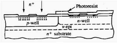
Explain the twin tub process with a neat diagram.
March 05, 2024
Twin-tub process:
Step 1:
n- Substrate is taken initially, which is shown in figure.
Step 2:
Next step is epitaxial layer deposition. Lightly doped epitaxial layer is deposited above nsubstrate.
Step 3:
The next step is tub formation. Two wells are formed namely n-well and p-well.
Polysilicon layer is formed above overall substrate.
Step 4:
Polysilicon gates are formed for n-well and p-well by using photo-etching process.
Step 5:
n+ diffusion is formed in n-well, P+ diffusion is formed in p-well. These are used for VDD contact and VSS contact. These are known as substrate formation.
Step 6:
Then, contact cuts are defined as in n-well process. Then metallization is processed.
 |
| Twin-tub process |

