Low Power Design Principles / Reducing dynamic power dissipation
March 14, 2024
- Explain various ways to minimize the static and dynamic power dissipation.
- Discuss the low power design principles in detail.
Low power design involves considering and reducing each of the terms in switching power.
i. As VDD is a quadratic term, it is good to select the minimum VDD.
ii. Choose the lowest frequency.
iii. The activity factor is reduced by putting unused blocks to sleep.
iv. Finally, the circuit may be optimized to reduce the overall load capacitance.
Switching power is consumed by delivering energy to charge a load capacitance, then dumping this energy to GND.
Activity factor:
- If a circuit can be turned OFF entirely, the activity factor and dynamic power go to zero.
- Blocks are typically turned OFF, by stopping the clock called as clock gating.
- The activity factor of a logic gate can be estimated by calculating the switching probability.
(a)Clock gating:
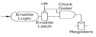
- Clock gating, AND’s a clock signal with an enable to turn OFF the clock to idle blocks.
- The clock enable must be stable, while the clock is active.
- Figure shows how an enable latch can be used to ensure the enable does not change before the clock falls.
Capacitance:
- Switching capacitance comes from the wires and transistors in a circuit.
- Wire capacitance is minimized through good floor planning and placement.
- Device-switching capacitance is reduced by choosing smaller transistors.
Voltage:
- Voltage has a quadratic effect on dynamic power.
- Therefore, choosing a lower power supply significantly reduces power consumption.
- The chip may be divided into multiple voltage domains, where each domain is optimized for the needs of certain circuits.
a. Voltage domains:
- Selecting, which circuits belong in which domain and routing power supplies to multiple domains.
- Figure (Voltage domain crossing) shows direct connection of inverters in two
- domains using high and low supplies, VDDH and VDDL, respectively.
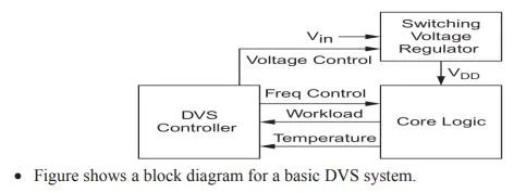
b. Dynamic voltage scaling (DVS):
- Systems can save large amounts of energy by reducing the clock frequency, then reducing the supply voltage.
- This is called dynamic voltage scaling (DVS) or dynamic voltage/frequency scaling (DVFS).
- It determines the supply voltage and clock frequency sufficient to complete the workload on schedule or to maximize performance without overheating.
Frequency:
- Dynamic power is directly proportional to frequency, so a chip should not run faster than necessary.
- Reducing the frequency allows downsizing transistors or using a lower supply voltage.
Low Power Architecture
- Device Level
- Low Capacitance in device and Multi Threshold Devices
- DVFS – Dynamic Voltage Frequency Scaling
- Multi VDD
- Gate Sizing
- Voltage Islands
- Power Gating
- Clock Gating
- Parallelism and Pipelined micro-architecture
Parallel Computations
• Multiple cores
• Multiple Issue pipelines
• Linear power increase
Pipelining
• Faster clock
• Exponential power increase
• Longer branch miss-predictions


