- Briefly discuss about the classification of circuit families and comparison of the circuit families.
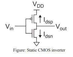
- Draw and explain the function of static CMOS
Static CMOS
Static CMOS circuits with complementary nMOS pulldown and pMOS pullup networks are used for the majority of logic gates in integrated circuits.
 |
| Static CMOS inverter |
Advantages of static CMOS:
- Static CMOS circuits have good noise margins
- Static CMOS circuits are fast, low power, easy to design.
- Static CMOS circuits are widely supported by CAD tools.
- Static CMOS circuits are available in standard cell libraries.
Drawback of static CMOS
- It requires both nMOS and pMOS transistors for each input.
- It has a relatively large logical effort.
- Gate delay is increased.
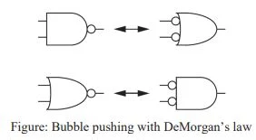
a. Bubble pushing
- CMOS stages are inherently inverting, so AND and OR functions must be built from NAND and NOR gates.
- DeMorgan’s law helps with this conversion:
 |
| Bubble pushing with DeMorgan’s law |
- A NAND gate is equivalent to an OR of inverted inputs.
- A NOR gate is equivalent to an AND of inverted inputs.
- The same relationship applies to gates with more inputs.
- Switching between these representations is easy and is often called bubble pushing.
b. Compound Gates
- Static CMOS also efficiently handles compound gates computing various inverting combinations of AND/OR functions in a single stage.
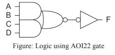
- The function F = AB +CD can be computed with an AND-OR INVERT- 22 (AOI22) gate and an inverter, as shown in Figure.
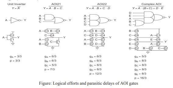
- Logical effort of compound gates can be different for different inputs.
- Figure shows, how logical efforts can be estimated for the AOI21, AOI22 and a more complex compound AOI gate.
- Design a circuit described by the Boolean function Y=[A.(B+C)(D+E)]’using CMOS logic.
 |
| Logical efforts and parasitic delays of AOI gates |
c. Input ordering delay effect
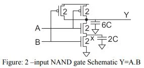
- The logical effort and parasitic delay of different gate inputs are different.
- Consider the falling output transition occurring, when one input hold a stable 1 value and the other rises from 0 to 1.
- If input B rises last, node x will initially be at VDD – Vt = VDD, because it was pulled up through the nMOS transistor on input A.
- The Elmore delay is (R/2)(2C) + R(6C) =7RC=2.33 τ
- If input A raises last, node x will initially be at 0 V, because it was discharged through the nMOS transistor on input B.
- No charge must be delivered to node x, so the Elmore delay is simply R(6C) =6RC =2τ.
- We define the outer input to be the input closer to the supply rail (e.g., B) and the inner input to be the input closer to the output (e.g., A).
- Therefore, if one signal is known to arrive later than the others, the gate is faster when that signal is connected to the inner input.
d. Asymmetric gates
- When one input is far less critical than another, even symmetric gates can be made asymmetric to favor the late input at the expense of the early one.
- In a series network, this involves connecting the early input to the outer transistor and making the transistor wider, so that, it offers less series resistance when the critical input arrives.
- In a parallel network, the early input is connected to a narrower transistor to reduce the parasitic capacitance.
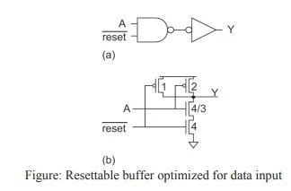
- Consider the path in Figure (a). Under ordinary conditions, the path acts as a buffer between A and Y.
- When reset is asserted, the path forces the output low.
- If reset only occurs under exceptional circumstances and take place slowly, the circuit should be optimized for input-to-output delay at the expense of reset.
- This can be done with the asymmetric NAND gate in Figure (b).
