Design a circuit described by the Boolean function Y=[A.(B+C)(D+E)]’using CMOS logic.
March 12, 2024
- Design a circuit described by the Boolean function Y=[A.(B+C)(D+E)]’using CMOS logic.
 |
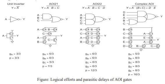
| Logical efforts and parasitic delays of AOI gates |
c. Input ordering delay effect
- The logical effort and parasitic delay of different gate inputs are different.
- Consider the falling output transition occurring, when one input hold a stable 1 value and the other rises from 0 to 1.
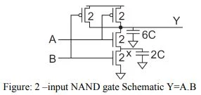
- If input B rises last, node x will initially be at VDD – Vt = VDD, because it was pulled up through the nMOS transistor on input A.
- The Elmore delay is (R/2)(2C) + R(6C) =7RC=2.33 τ
- If input A raises last, node x will initially be at 0 V, because it was discharged through the nMOS transistor on input B.
- No charge must be delivered to node x, so the Elmore delay is simply R(6C) =6RC =2τ.
- We define the outer input to be the input closer to the supply rail (e.g., B) and the inner input to be the input closer to the output (e.g., A).
- Therefore, if one signal is known to arrive later than the others, the gate is faster when that signal is connected to the inner input.
d. Asymmetric gates
- When one input is far less critical than another, even symmetric gates can be made asymmetric to favor the late input at the expense of the early one.
- In a series network, this involves connecting the early input to the outer transistor and making the transistor wider, so that, it offers less series resistance when the critical input arrives.
- In a parallel network, the early input is connected to a narrower transistor to reduce the parasitic capacitance.
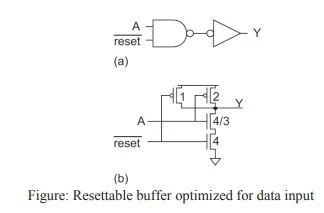
- Consider the path in Figure (a). Under ordinary conditions, the path acts as a buffer between A and Y.
- When reset is asserted, the path forces the output low.
- If reset only occurs under exceptional circumstances and take place slowly, the circuit should be optimized for input-to-output delay at the expense of reset.
- This can be done with the asymmetric NAND gate in Figure (b).


