CMOS DEVICES & TECHNOLOGIES
The four main CMOS technologies are
n-Well process
p-Well process
Twin-tub Process
Silicon on Insulator
Explain the different steps involved in CMOS fabrication / manufacturing process with neat diagrams. (Nov 2007, Nov 2009, Nov 2016, NOV 2018)
Describe with neat diagram the n-well and channel formation in CMOS process. (Nov/Dec 2014)(Nov/Dec 2011) (April/May 2011) (Nov/Dec 2012)
n-WELL PROCESS:
Step 1: Start with blank wafer
First step will be to form the n-well
– Cover wafer with protective layer of SiO2 (oxide)
– Remove layer where n-well should be built.
Step 2: Oxidation
Grow SiO2 on top of Si wafer, at 900 – 12000 C with H2O or O2 in oxidation furnace.
Step 3: Photoresist
• Spin on photoresist
– Photoresist is a light-sensitive organic polymer.
– Softens, where exposed to light.
Step 4: Lithography
• Expose photoresist through n-well mask.
• Strip off exposed photoresist.
Step 5: Etch
• Etch oxide with hydrofluoric acid (HF).
• Only attracts oxide, where resist has been exposed.
Step 6: Strip Photoresist
• Etch the remaining photoresist using a mixture of acids.

Step 7: n-well
n-well is formed with diffusion or ion implantation.
Step 8: Strip Oxide
• Strip off the remaining oxide using HF.
• Back to bare wafer with n-well.
• Subsequent steps involve similar series of steps.
Step 9: Polysilicon
• Deposit thin layer of oxide. Use CVD to form poly and dope heavily to increase conductivity.
Step 10: Polysilicon Patterning
• Use same lithography process to pattern polysilicon.
Step 11: Self-Aligned Process
Cover with oxide to define n diffusion regions.
Step 12: N-diffusion
• Pattern oxide, using n+ active mask to define n diffusion regions.
• Diffusion or ion implantation is used to create n diffusion regions.
Step 13:
• Strip off oxide to complete patterning step.
Step 14: P-Diffusion
• Similar set of steps are followed to form p+ diffusion regions for pMOS source and drain and substrate contact.
Step 15: Contacts
• Now, we need to wire together the devices.
• Cover chip with thick field oxide.
• Etch oxide, where contact cuts are needed.
Step 16: Metallization
• Sputter on aluminum over whole wafer.
• Pattern to remove excess metal, leaving wires.
P-WELL PROCESS:
A common approach to p-well CMOS fabrication is to start with moderately doped n-type substrate (wafer), create the p-type well for the n-channel devices and build the p-channel transistor in the native n-substrate.
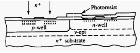
Explain the twin tub process with a neat diagram. (Nov 2007, April 2008)
Twin-tub process:
Step 1:
n- Substrate is taken initially, which is shown in figure.
Step 2:
Next step is epitaxial layer deposition. Lightly doped epitaxial layer is deposited above nsubstrate.
Step 3:
The next step is tub formation. Two wells are formed namely n-well and p-well.
Polysilicon layer is formed above overall substrate.
Step 4:
Polysilicon gates are formed for n-well and p-well by using photo-etching process.
Step 5:
n+ diffusion is formed in n-well, P+ diffusion is formed in p-well. These are used for VDD contact and VSS contact. These are known as substrate formation.
Step 6:
Then, contact cuts are defined as in n-well process. Then metallization is processed.
 |
| Twin-tub process |


