Delay estimation
March 10, 2024
Draw a CMOS inverter. Analyze the switching characteristics during rise time when Vin change from high to low.
Derive an expression for the rise time, fall time and propagation delay of a CMOS inverter.
Important definitions for delay estimation:
Propagation delay time (tpd):
Propagation delay time is defined as maximum time from the input crossing 50% to the output crossing 50%.
Contamination delay time (tcd):
Contamination delay time is defined as minimum time from the input crossing 50% to the output crossing 50%.
Rise time (tr):
Rise time is defined as time for a waveform to rise from 20% to 80% of its steady-state value
Fall time (tf):
Fall time is defined as time for a waveform to fall from 80% to 20% of its steady-state value.
Edge rate is average of rise and fall time, ( trf) = (tr + tf )/2 Delay estimation.
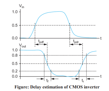
Delay estimation response curve:
- When an input changes, the output will retain its old value for at least the contamination delay and take on its new value in, at most the propagation delay.
- Delays for the output rising is tpdr /tcdr and the output falling is tpdf /tcdf .
- Rise/fall times are also called as slopes or edge rates.
- Propagation and contamination delay times are also called as max-time and min-time respectively.
 |
| Delay estimation of CMOS inverter |
- The gate that charges or discharges a node is called the driver. The gates and wires being driven, are called the load. Propagation delay is usually called as delay.
- Arrival times and propagation delays are defined separately for rising and falling transitions.
- The delay of a gate may be different from different inputs. Earliest arrival times can also be computed based on contamination delays.
- Expression of delay for rising output is tPLH = 0.69 RP.CL
Where, RP – effective resistance of pMOS transistor
CL - load capacitance of CMOS inverter.
- Expression of delay for falling output is tPHL = 0.69 RN.CL
Where, RN – effective resistance of nMOS transistor
- Propagation delay of CMOS inverter is tP = (tPLH + tPHL) / 2

