Elmore’s Delay
March 11, 2024
- What is meant by Elmore’s delay and give expression for Elmore’s delay?
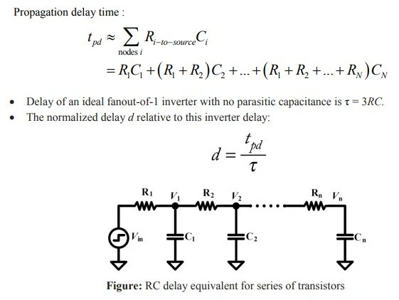
The Elmore delay model estimates the delay from a source, switching to one of the leaf nodes. Delay is the sum over each node i of the capacitance Ci on the node multiplied by the effective resistance R.
 |
| RC delay equivalent for series of transistors |
Linear delay model
- The RC delay model is one, where delay is a linear function of the fanout of a gate.
- The normalized delay of a gate can be expressed in units of Y as d = f + p.
- Where p is the parasitic delay inherent to the gate when no load is attached.
f is the effort delay or stage effort that depends on the complexity.
Effort delay of the gate is f = gh.
- Where g is the logical effort (An inverter has a logical effort of 1).
- Logical effort is defined as the ratio of the input capacitance of a gate to the input capacitance of an inverter delivering the same output current.
- h is the fanout or electrical effort. Electrical effort is defined as ratio of the output capacitance to input capacitance.
- More complex gates have greater logical efforts, indicating that they take longer time to drive a given fanout.
- For example, the logical effort of the 3-input NAND gate is 5/3.
- The electrical effort can be computed as h= Cout in / Cin
- Where Cout is the capacitance of the external load being driven and Cin is the capacitance of the gate.
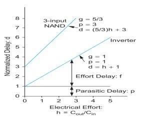
- Normalized delay vs electrical effort for an idealized inverter and 3-input NAND gate shown in diagram.
- The y-intercepts indicate the parasitic delay. The slope of the lines is the logical effort.
- The inverter has a slope of 1. The NAND gate has a slope of 5/3.
Design a four input NAND gate and obtain its delay during the transition from high to low.
Figure shows a model of an n-input NAND gate in which the upper inputs were all 1 and the bottom input rises. The gate must discharge the diffusion capacitances of all of the internal nodes as well as the output.
Elmore delay is


