
Logical effort
- Obtain the logical effort and path efforts of the given circuit.
Delay in Multistage Logic Networks:
The figure shows the logical and electrical efforts of each stage in a multistage path as a function of the sizes of each stage.
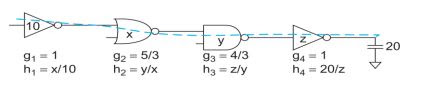
The path of interest (the only path in this case) is marked with the dashed blue line. Observe that logical effort is independent of size, while electrical effort depends on sizes.
The path logical effort G can be expressed as the products of the logical efforts of each stage along the path.

The product of the stage efforts is F, independent of gate sizes. The path effort delay is the sum of the stage efforts. The sum of a set of numbers whose product is constant is minimized by choosing all the numbers to be equal.
The path delay is minimized when each stage bears the same effort. If a path has N stages and each bears the same effort, that effort must be
fˆ = gi hi = F 1 / N
Thus, the minimum possible delay of an N-stage path with path effort F and path
parasitic delay P is
D = NF 1/ N + P
It shows that the minimum delay of the path can be estimated knowing only the number of stages, path effort, and parasitic delays without the need to assign transistor sizes.
The capacitance transformation formula is used to find the best input capacitance for a

gate given the output capacitance it drives.
At the end of the path, apply the capacitance transformation to determine the size of each stage. Check the arithmetic by verifying that the size of the initial stage matches the specification.
