pseudo nMOS
March 12, 2024
- Explain the detail about pseudo-nMOS gates with neat circuit diagram.
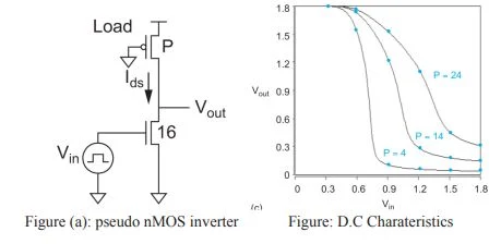
- Figure (a) shows a pseudo-nMOS inverter.
- The static load is built from a single pMOS transistor that has its gate grounded, so it is always ON.
- The beta ratio affects the shape of the transfer characteristics and the VOL of the inverter.
- Larger relative pMOS transistor size offer faster rise time, but less sharp transfer characteristics.
- Drawback: Pseudo-nMOS gates will not operate correctly if VOL >VIL of the receiving gate.
Figure shows several pseudo-nMOS logic gates.


