Skewed gates
March 12, 2024
- What is meant by skewed gate and give functions of skewed gate with schematic diagrams?
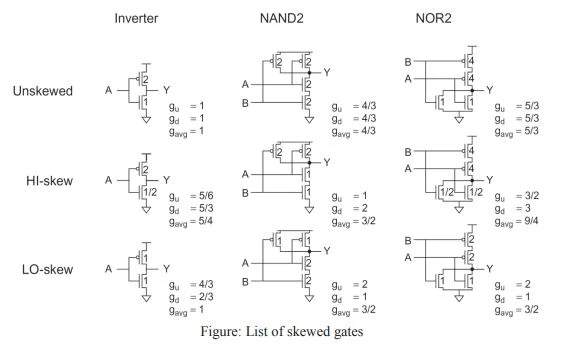
- One input transition is more important than the other. HI-skew gates to favor the rising output transition. LO-skew gates to favor the falling output transition.
- This favoring can be done by decreasing the size of the noncritical transistor.
- The logical efforts for the rising (up) and falling (down) transitions are called gu and gd, respectively.
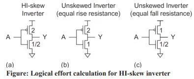
- Figure (a) shows, how a HI-skew inverter is constructed by downsizing the nMOS transistor.
- This maintains the same effective resistance for the critical transition, while reducing the input capacitance relative to the unskewed inverter of Figure (b).
- Thus reducing the logical effort on that critical transition to gu = 2.5/3 =5/6.
- The logical effort for the falling transition is estimated by comparing the inverter to a smaller unskewed inverter with equal pulldown current, shown in Figure (c), giving a logical effort of gd =2.5/1.5 =5/3.
- Figure shows, HI skew and LO-skew gates with a skew factor of two. Skewed gates are sometimes denoted with an H or an L on their symbol in a schematic.
 |
| List of skewed gates |
f. P/N ratios
- By accepting a slower rise delay, the pMOS transistors can be downsized to reduce input capacitance and average delay significantly.
- P/N ratio is defined as the ratio of pMOS to nMOS transistor width. For processes, a mobility ratio of µn/µp = 2
g. Multiple threshold voltages
- Some CMOS processes offer two or more threshold voltages.
- Transistors with lower threshold voltages produce more ON current, but also leak
- exponentially more OFF current.
- Libraries can provide both high- and low-threshold versions of gates.
- The low-threshold gates can be used carefully to reduce the delay of critical paths.
- Skewed gates can use low-threshold devices on, only the critical network of transistors.


