MOS(FET) Transistor Characteristic under Static and Dynamic Conditions
March 05, 2024
Explain the DC transfer characteristic of CMOS inverter.[APRIL-2015, Nov 2015]
Draw and explain the DC and transfer characteristics of a CMOS inverter with necessary conditions for the different regions of operation. (Nov/Dec 2011) (Nov/Dec 2012) (May/June 2013) (April/May 2012) (May/June 2014) (Nov/Dec 2013) (May 2016, May 2017, Nov 2008) [April/May-2022.] [Nov/Dec-2020., April/May-2021] [April/May 2023]
Explain the CMOS inverter DC characteristics. (Nov 2007, Nov 2009) [Nov/Dec 2022]
The DC transfer characteristics of a circuit relate the output voltage to the input voltage.
(i) Static CMOS inverter DC Characteristics:
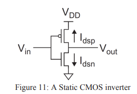
The DC transfer function (Vout Vs. Vin) for the static CMOS inverter shown in Figure 11.
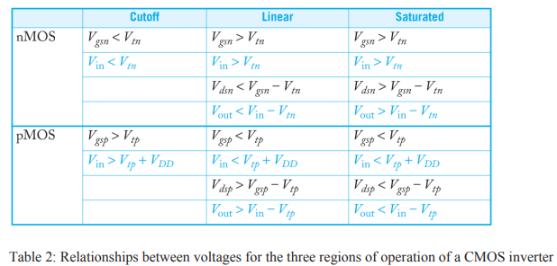
- Table 2, shows various regions of operation for the n and p transistors.
- In this table, Vtn is the threshold voltage of the n-channel device, and Vtp is the threshold voltage of the p-channel device. Vtp is negative.
- The equations are given both in terms of Vgs /Vds and Vin /Vout.
- As the source of the nMOS transistor is grounded, Vgsn = Vin and Vdsn = Vout.
- As the source of the pMOS transistor is tied to VDD, Vgsp = Vin – VDD and Vdsp = Vout – VDD.
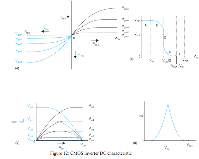
- Figure 12(a), shows Idsn and Idsp in terms of Vdsn and Vdsp for various values of Vgsn and Vgsp.
- Figure 12(b), shows the same plot of Idsn and |Idsp| in terms of Vout for various values of Vin.
- Operating points are plotted on Vout vs. Vin axes in Figure 12(c) to show the inverter DC transfer characteristics.
- The supply current IDD = Idsn = |Idsp| is plotted against Vin in Figure 13(d) showing that both transistors are momentarily ON as Vin.
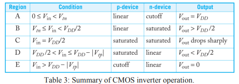
- The operation of the CMOS inverter can be divided into five regions as indicated on figure 12(c).
The state of each transistor in each region is shown in Table 3.
- In region A, the nMOS transistor is OFF and the pMOS transistor pulls the output to VDD.
- In region B, the nMOS transistor starts to turn ON. It is pulling the output down.
- In region C, both transistors are in saturation.
- In region D, the pMOS transistor is partially ON.
- In region E, PMOS is completely OFF, making the nMOS transistor to pull the output down to GND.
(ii) Beta ratio Effects:
- For βp = βn, the inverter threshold voltage Vinv is VDD/2.
- It allows a capacitive load to charge and discharge in equal times by providing equal current source and equal sink capabilities.
- Inverter with different beta ratios r = βp /βn is called skewed inverter.
- If r > 1, the inverter is HI-skewed. If r < 1, the inverter is LO-skewed. If r = 1, the inverter has normal skew or is unskewed.
- Figure 13, shows the impact of skewing the beta ratio on the DC transfer characteristics.
- As the beta ratio is changed, the switching threshold is varied.
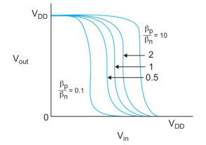 |
| Transfer characteristics of skewed inverters |
(iii) Noise Margins:
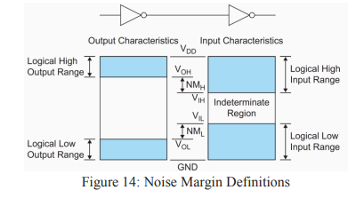
- Noise margin (Noise immunity) is related to the DC voltage characteristics.
- Noise Margin allows determining the allowable noise voltage on the input of a gate, so that the output will not be corrupted.
- Two parameters of the noise margin are LOW noise margin (NML), and the HIGH noise margin (NMH).
- NML is defined as the difference in maximum LOW input voltage VIL and the maximum LOW output voltage VOL. NML = VIL - VOL
- The value of NMH is the difference between the minimum HIGH output voltage VOH and the minimum HIGH input voltage VIH. i.e., NMH = VOH - VIH
- Inputs between VIL and VIH are said to be in the indeterminate region or forbidden zone.
(iv) Pass Transistor DC Characteristics:
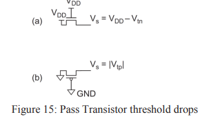
- The nMOS transistors pass 0’s well but 1’s poorly. Figure 15(a), shows an nMOS transistor with the gate and drain tied to VDD.
- Initially at Vs = 0. Vgs > Vtn, so the transistor is ON and current flow.
- Therefore, nMOS transistors attempting to pass a 1 never pull the source above VDD – Vtn. This loss is called a threshold drop.
- The pMOS transistors pass 1’s well but 0’s poorly.
- If the pMOS source drops below |Vtp|, the transistor cuts off.
- Hence, pMOS transistors only pull down to a threshold above GND, as shown in Figure 15(b).
Tags

