NON IDEAL I-V EFFECTS
March 05, 2024
Explain in detail about the non ideal I-V characteristics of a CMOS device. (MAY 2013)
Explain channel length modulation and body effect. (Nov 2009, May 2013)
MOS characteristics degrade with temperature. It is useful to have a qualitative understanding of non ideal effects to predict their impact on circuit behavior.
(i) Mobility Degradation and Velocity Saturation:
- Current is proportional to the lateral electric field Elat = Vds /L between source and drain.
- A high voltage at the gate of the transistor attracts the carriers to the edge of the channel, causing carriers collision with the oxide interface that slows the carriers. This is called mobility degradation.
- Carriers approach a maximum velocity (vsat) when high fields are applied. This phenomenon is called velocity saturation.
(ii) Channel Length Modulation:
- Current Ids is an independent of Vds for a transistor in saturation.
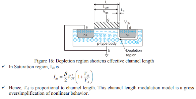
- The p–n junction between the drain and body forms a depletion region with a width Ld that increases with Vdb , as shown in Figure 16.
- The depletion region effectively shortens the channel length to Leff = L - Ld
- To avoid the body voltage into calculations, assume the source voltage is close to the body voltage i.e Vdb = Vds.
- Hence, increasing Vds decreases the effective channel length.
- Shorter channel length results in higher current. Thus, Ids increases with Vds in saturation, as shown in Figure 16.
 |
| Depletion region shortens effective channel length |
(iii) Threshold Voltage (Vt) Effects
Explain in detail about effect and its effect in MOS device. (May 2016)
Threshold voltage Vt increases with the source voltage, decreases with the body voltage, decreases with the drain voltage and increases with channel length.
Body Effect:
- When a voltage Vsb is applied between the source and body, it increases the amount of charge required to invert the channel. Hence, it increases the threshold voltage.
- The threshold voltage can be modeled as
(iv) Leakage:
- Even when transistors are OFF, transistors leak small amounts of current.
- Leakage mechanisms include subthreshold conduction between source and drain, gate leakage from the gate to body and junction leakage from source to body and drain to body.
- Sub threshold conduction is caused by thermal emission of carriers over the potential barrier set by the threshold.
- Gate leakage is a quantum-mechanical effect caused by tunneling through the extremely thin gate dielectric.
- Junction leakage is caused by current through the p-n junction between the source/drain diffusions and the body.
Tags


