
C – V CHARACTERISTICS OF MOS TRANSISTOR (AC characteristics)
March 04, 2024
Explain the dynamic behavior of MOSFET transistor with neat diagram. (April 2018)
Discuss the CV characteristics of the CMOS. (Nov 2012, May 2014, Nov 2015, Nov 2016)
Explain the electrical properties CMOS. (Nov 2017) [April / May 2023]
Each terminal of an MOS transistor has capacitance to the other terminals. Capacitances are nonlinear and voltage dependent (C-V).
SIMPLE MOS CAPACITANCES MODEL:
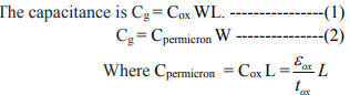
- The gate of an MOS transistor is a good capacitor. Its capacitance is necessary to attract charge to invert the channel, so high gate capacitance is required to obtain high Ids.
- The gate capacitor can be viewed as a parallel plate capacitor with the gate on top, channel on bottom and the thin oxide dielectric between.
- In addition to the gate, the source and drain also have capacitances. These capacitances are called parasitic capacitors.
- The source and drain capacitances arise from the p–n junctions between the source or drain diffusion and the body. These capacitances are called diffusion capacitance Csb and Cdb.
- The depletion region acts as an insulator between the conducting p- and n-type regions, creating capacitance across the junction.
- The capacitance of junctions depends on the area and perimeter of the source and drain diffusion, the depth of the diffusion, the doping levels and the voltage.
- As diffusion has both high capacitance and high resistance, it is generally made as small as possible in the layout.
DETAILED MOS GATE CAPACITANCE MODEL:
- MOS gate places above the channel and may partially overlap the source and drain diffusion areas.
- The gate capacitance has two components, (i) the intrinsic capacitance Cgc (over the channel) and (ii) the overlap capacitances Cgol (to the source and drain).
- The intrinsic capacitance was approximated as a simple parallel plate with capacitance
- C0 =WLCox.
- The intrinsic capacitance has three components representing the different terminals connected to the bottom plate are Cgb (gate-to-body), Cgs (gate-to-source), and Cgd (gate-to-drain).
- The behavior in three regions (Cutoff, Linear and Saturation) can be approximated as shown in Table 1.


DETAILED MOS DIFFUSION CAPACITANCE MODEL:
- The capacitance depends on both the area AS and sidewall perimeter PS of the source diffusion region. The area is AS = WD.
- The perimeter is PS = 2W +2D.
 |
| Diffusion region geometry |
- The total source parasitic capacitance is Csb = AS * C jbs + PS* C jbssw
- Where, Cjbs - Capacitance of the junction between the body and the bottom of the source Cjbssw - Capacitance of the junction between the body and the side walls of the source
- In summary, MOS transistor can be viewed as a four-terminal device with capacitances between each terminal pair, as shown in Figure 10.
 |
| Capacitance of a MOS Transistor |
- The gate capacitance includes an intrinsic component and overlap terms with the source and drain. The source and drain have parasitic diffusion capacitance to the body.
Tags
