Latchup problem
March 10, 2024
- Discuss the origin of latch up problems in CMOS circuits with necessary diagrams. Explain the remedial measures.
- A CMOS process is slowed down by developing low-resistance paths between VDD and GND, causing catastrophic meltdown. The phenomenon is called latchup.
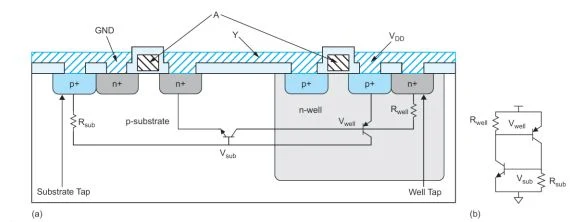
- Latchup problem arises when parasitic bipolar transistors are formed by the substrate, well and diffusion.
- The cause of the latchup effect can be understood by examining the process cross-section of a CMOS inverter, as shown in Figure (a).
- The schematic shows, a circuit composed of an npn-transistor, a pnp-transistor, and two resistors connected between the power and ground rails (Figure (b)).
 |
| latch up problems in CMOS circuits |
- The npn transistor is formed between the grounded n-diffusion source of the nMOS transistor, the p-type substrate and the n-well.
- The resistors are due to the resistance through the substrate or well to the nearest substrate and well taps.
- The cross-coupled transistors form a bistable silicon-controlled rectifier (SCR). Both parasitic bipolar transistors are OFF.
- Latchup can be triggered, when transient currents flow through the substrate during normal chip power-up.
- Latchup prevention is easily accomplished by
- Minimizing Rsub and Rwell.
- Use of guard rings
- SOI process avoids latchup entirely, because they have no parasitic bipolar structures.

