- Explain about stick diagram in VLSI design.
- Draw the static diagram of CMOS inverter.
- A stick diagram is a cartoon of a chip layout. A "stick diagram" is a paper and pencil tool that use to plan the layout of a cell.
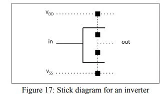
- The stick diagram resembles the actual layout, but uses "sticks" or lines to represent the devices and conductors. Figure 17, shows a stick diagram for an inverter.
- The stick diagram represents the rectangles with lines, which represent wires and component symbols.
- The stick diagram does not represent all the details of a layout, but it makes some relationship much clearer and it is simple to draw.
- Layouts are constructed from rectangles, but stick diagrams are built from cartoon symbols for components and wires.
Stick diagram Rules:
- Rule 1: When two or more ‘sticks’ of the same type cross or touch each other, that
- represents electrical contact.
- Rule 2: When two or more ‘sticks’ of the different type cross or touch each other, there is no electrical contact. If electrical contact is needed, we have to show the connection explicitly.
- Rule 3: When a poly crosses diffusion, it represents a transistor. If a contact is shown, then it is not a transistor. A transistor exists where a polysilicon (red) stick crosses either an ndiffusion (green) stick or a p-diffusion (yellow) stick.
- Rule 4: In CMOS, a demarcation line is drawn to avoid touching of p-diff with n-diff. All pMOS must lie on one side of the line and all nMOS will have to be on the other side.
 |
| Stick diagram for an inverter |
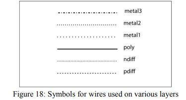
The symbols for wires used on various layers are shown in Figure 18
 |
| Symbols for wires used on various layers |
Drawing stick diagrams in color:
- Red for poly, green for n-diffusion, yellow for p-diffusion, and shades of blue for metal are typical colors.
- A few simple rules for constructing wires from straight-line segments ensure that, the stick diagram corresponds to a feasible layout.
- Wires cannot be drawn at arbitrary angles. Only horizontal and vertical wire segments are allowed.
- Two wire segments on the same layer, which cross are electrically connected.
- Vias to connect wires, which do not normally interact, are drawn as black dots.
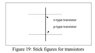
- Figure 19, shows the stick figures for transistors.
- Each type of transistor is represented as poly and diffusion crossings, much as in the layout.
 |
| Stick figures for transistors |
- Area and aspect ratio are also difficult to estimate from stick diagrams.
- Stick diagrams are especially important tools for layouts built from large cells and for testing the connections between cells.
