- Describe the basic principle of operation of dynamic CMOS, domino and NP domino logic with neat diagrams.
- Ratioed circuits reduce the input capacitance by replacing the pMOS transistors connected to the inputs with a single resistive pullup.
- The drawbacks of ratioed circuits include
- Slow rising transitions,
- Contention on the falling transitions,
- Static power dissipation and a nonzero VOL.
- Dynamic circuits avoid these drawbacks by using a clocked pullup transistor rather than a pMOS that is always ON.
- Figure compares (a) static CMOS, (b) pseudo-nMOS, and (c) dynamic inverters.
%20static%20CMOS,%20(b)%20pseudo-nMOS,%20and%20(c)%20dynamic%20inverters.JPG) |
| Comparison of (a) static CMOS, (b) pseudo-nMOS, and (c) dynamic inverters |
Dynamic circuit operation is divided into two modes, as shown in Figure.
(i) During precharge, the clock ф is 0, so the clocked pMOS is ON and initializes the output Y high.
(ii) During evaluation, the clock is 1 and the clocked pMOS turns OFF. The output may remain high or may be discharged low through the pulldown network.
Advantages:
- Dynamic circuits are the fastest used circuit family because they have lower input capacitance and no contention during switching.
- Zero static power dissipation.
Disadvantages:
- They require careful clocking, consume significant dynamic power and are sensitive to noise during evaluation mode.
Foot transistor:
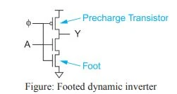
- In Figure (c), if the input A is 1 during precharge, contention will take place because both the pMOS and nMOS transistors will be ON.
- When the input cannot be guaranteed to be 0 during precharge, an extra clocked evaluation transistor can be added to the bottom of the nMOS stack.
- To avoid contention as shown in the below figure, extra transistor is sometimes called as foot is added.
 |
| Footed dynamic inverter |
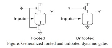
- The given below figure shows generic footed and unfooted gates.
 |
| Generalized footed and unfooted dynamic gates |
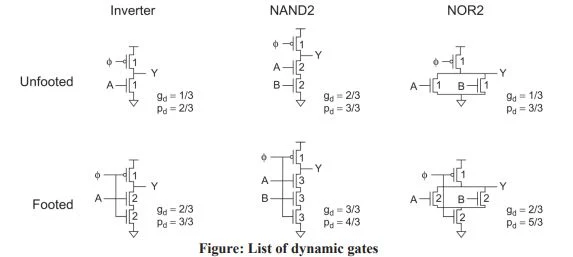
- The given below figure estimates the falling logical effort of both footed and unfooted dynamic gates.
 |
| List of dynamic gates |
- The pull down transistor’s width is chosen to give unit resistance. Precharge occurs while the gate is idle and takes place more slowly.
- Therefore, the precharge transistor width is chosen for twice unit resistance.
- This reduces the capacitive load on the clock and the parasitic capacitance at the expense of greater rising delays.
- Footed gates have higher logical effort than their unfooted concept but are still an
- improvement over static logic.
- The parasitic delay does increase with the number of inputs, because there is more diffusion capacitance on the output node.
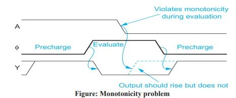
- A fundamental difficulty with dynamic circuits is the monotonicity requirement. While a dynamic gate is in evaluation, the inputs must be monotonically rising.
- That is, the input can start LOW and remain LOW, start LOW and rise HIGH, start HIGH and remain HIGH, but not start HIGH and fall LOW.
- Figure shows waveforms for a footed dynamic inverter in which the input violates monotonicity.
 |
| Monotonicity problem |
- During precharge, the output is pulled HIGH.
- When the clock rises, the input is HIGH, so the output is discharged LOW through the pulldown network.
- The input later falls LOW, turning off the pulldown network. However, the precharge transistor is also OFF, so the output floats, staying LOW rather than rising.
- The output will remain low until the next precharge step.
- The inputs must be monotonically rising for the dynamic gate to compute the correct function.
- Unfortunately, the output of a dynamic gate begins HIGH and monotonically falls LOW during evaluation.
- This monotonically falling output X is not a suitable input to a second dynamic gate expecting monotonically rising signals, as shown in the below figure.
- Dynamic gates sharing the same clock cannot be directly connected.
- This problem is often overcome with domino logic.
 |
| Incorrect connection of dynamic gates |
The charge sharing problem occurs when the charge which is stored at the output node in the pre-charge phase is shared among the junction capacitance of transistors in the evaluation phase. Charge sharing may degrade the output voltage level or even cause an erroneous output value.
To overcome the dynamic charge sharing and soft- node leakage problems in NORA CMOS structures, a circuit technique called Zipper CMOS can be used. The basic circuit architecture of Zipper CMOS is essentially identical to NORA CMOS, with the exception of the clock signals.
%20static%20CMOS,%20(b)%20pseudo-nMOS,%20and%20(c)%20dynamic%20inverters.JPG)
